University of California at Santa Barbara (UCSB) researchers have developed new nanoscale structures that will help to speed up computers. This research project was funded by IBM, Intel and other partners including the U.S. National Science Foundation. This new manufacturing process is called block co-polymer lithography (or BCP).
The scientists 'have created a way to make square, nanoscale, chemical patterns -- from the bottom up -- that may be used in the manufacture of integrated circuit chips as early as 2011.'
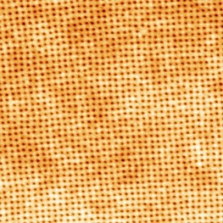
You can see above an atomic force microscope (AFM) image of a square array of 15nm pores formed by the new technology. (Credit: UCSB research team)
This new process for creating features on silicon wafers that are between five and 20 nanometers thick has been developed by a multidisciplinary team led by Craig Hawker, materials professor and director of the Materials Research Laboratory at UCSB and the members of his research group. Hawker worked with professors Glenn Fredrickson -- and his research group -- and Edward Kramer -- and his research group.
It's almost obvious that we will need more powerful microprocessors that use less energy in the future. Here are some quotes from Hawker about this. "'If you can shrink all these things down, you get both. You get power and energy efficiency in one package. [...] One of the problems is that the industry is now running into physical limitations. You can't shrink things down any more with the current technology.' One of the ways that microprocessors are made is by using a top-down technique called photolithography, which involves shining light onto the surface of a silicon wafer, and making patterns. He explained that the size of the wavelength of light is becoming a limiting factor, and so his team has invented a new way of creating smaller patterns."
Later, Hawker describes the BCP approach. "'We've come up with this new blending approach, called block co-polymer lithography, or BCP. It essentially relies on a natural self-assembly process. Just like proteins in the body, these molecules come together and self assemble into a pattern. And so we use that pattern as our lithographic tool, to make patterns on the silicon wafer.' Using this technique, the size of the features is about the same as that of the molecules. They are very small, between five and 20 nanometers. 'With this strategy, we can make many more features,' said Hawker, 'and hence we can pack the transistors closer together and everything else closer together –– using this new form of lithography.'"
This new process has been designed to be compatible with current manufacturing techniques, so semiconductor manufacturers could use it without losing their previous investments.
According to Hawker, the BCP process is similar to what you're doing in your kitchen when you are preparing a salad dressing. "'Think of the block co-polymers as oil and water. When you make salad dressing you shake up the bottle because the oil and water don't want to be together. They separate into two layers. You shake your salad dressing and you mix everything up into much smaller droplets. What we've done is taken two polymer molecules that hate each other and joined them together. And so they want to separate just like the oil and water in your salad dressing. But because we've molecularly joined them, they can't. And so they separate into very, very small droplets, or domains, based on the fact that they hate each other. Those are the BCPs.'"
In "Self-assembly goes square-shaped - physicsworld.com," Belle Dumé provides additional details on what is BCP (PhysicsWorld.com, September 27, 2008, free registration). "Self-assembled square arrays are a major goal for researchers because the semiconductor industry's circuit design, software and fabrication processes are all based on a rectilinear coordinate system. Although hexagonal patterns can now routinely be produced using conventional self-assembly techniques, adopting these shapes would mean rethinking semiconductor industry protocols, which would be very expensive and time-consuming. To this end, the Semiconductor Industry Association has set up a challenge to scientists working in the field of 'block copolymer' lithography to develop square arrays of etchable block copolymer domain patterns."
Here is a second quote from this article. "Block copolymer lithography is a simple approach to make features smaller than 20 nm, which is less than half the size of today’s smallest mass-produced circuits. Block copolymers are two different kinds of polymer strand (called blocks) that are joined end-to-end to create one long strand. Although the ends of the blocks are stuck together, the blocks tend to repel each other along their length. These competing forces tend to organize the copolymers into well defined patterns with length scales of tens of nanometers."
For even more information, this research work has been published in Science Express under the name "Evolution of Block Copolymer Lithography to Highly Ordered Square Arrays" on September 25, 2008. Here is the abstract. "The manufacture of smaller, faster and more efficient microelectronic components is a major scientific and technological challenge, driven in part by a constant need for smaller lithographically defined features and patterns. While traditional self-assembling approaches based on block copolymer lithography spontaneously form nanometer sized hexagonal structures, these features are not consistent with the industry standard rectilinear coordinate system. In this work, a modular and hierarchical self-assembly strategy, combining supramolecular assembly of hydrogen-bonding units with controlled phase separation of diblock copolymers, is presented for the generation of nanoscale square patterns. These square arrays hold particular promise for simplicity of addressability and circuit interconnection in integrated circuit manufacturing and nanotechnology."


No comments:
Post a Comment